This applet is an electronic circuit simulator written in Java by Paul Falstad and ported to JavaScript by Iain Sharp. When the applet starts up you will see a circuit which I've chosen to welcome you with. The green color indicates positive voltage. The gray color indicates ground. A red color indicates negative voltage. The moving yellow dots indicate current.
To turn a switch on or off, just click on it. If you move the mouse over any component of the circuit, you will see a short description of that component and its current state in the lower right corner of the window. To modify a component (say, to change the resistance of one of the resistors), move the mouse over it, click the right mouse button (or control-click, if you have a Mac) and select “Edit”.
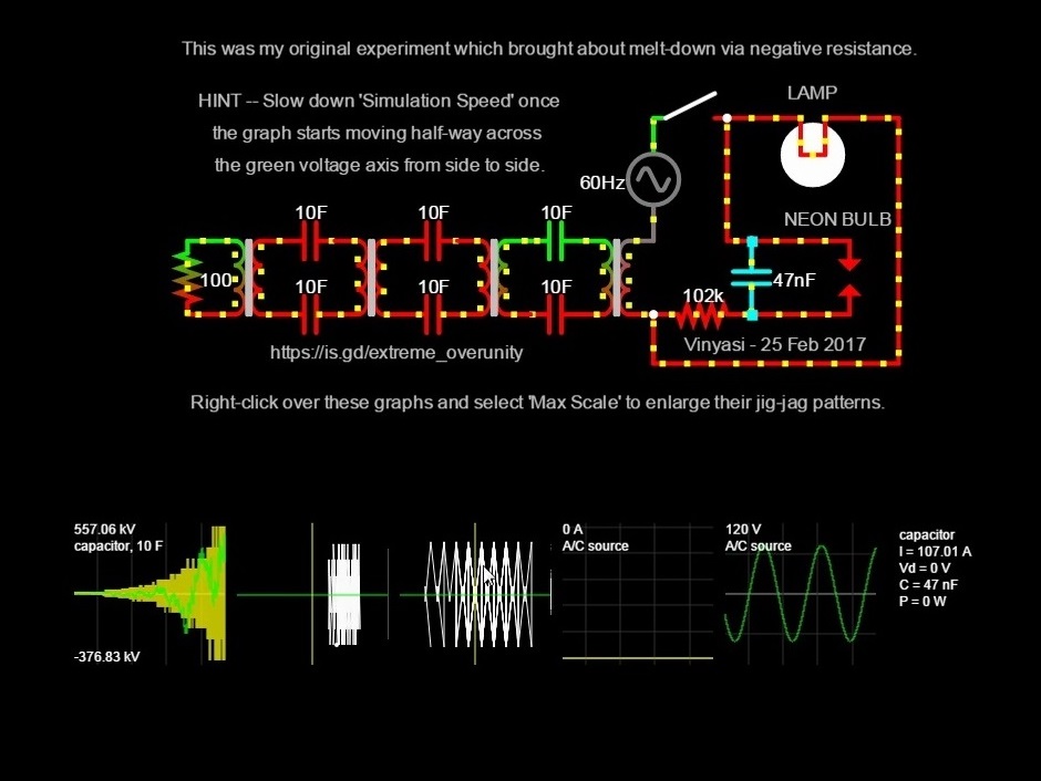
There are three graphs at the bottom of the window; these act like oscilloscopes, each one showing the voltage and current across a particular component. Voltage is shown in green, and current is shown in yellow. The current may not be visible if the voltage graph is on top of it. The peak value of the voltage in the scope window is also shown. Move the mouse over one of the scope views, and the component it is graphing will be highlighted. To modify or remove a scope, click the right mouse button over it. To view a component in the scope, click the right mouse button over the component and select “View in Scope”.
If the simulation is moving too slowly or too quickly, you can adjust the speed with the “Simulation Speed” slider.
Once you download a circuit, you can create a link, or bookmark, to an individual circuit of your choice by attaching its file name to the end of this link...
https://vinyasi.info/ne?startCircuit= + example-circuit.txt
For example: https://vinyasi.info/ne?startCircuit=chua.txt
Despite my usage of conventional terminology regarding NEGATIVE RESISTORS and NEGATIVE RESISTANCES, I will no longer use those terms, because I find them to be not accurate enough and a bit misleading. The correct term is RECIPROCAL RESISTANCE since Ohm's Law becomes the reciprocal of itself. Hence, instead of dividing voltage by resistance to get current in a normal resistor, Mho's Law would be its equivalent reciprocal by dividing resistance by voltage to get current in a reciprocal resistor. Positive and negative resistance is reserved for just that: a positive or negative value to a resistor measured in Ohm's. For example, see ...
https://vinyasi.info/ne?startCircuit=negrecipresist.txt
Transformers have also been revised to include the ability for increasing their coefficient of performance above unity and up to one billion.
https://vinyasi.info/ne?startCircuit=transformer.txt
And it's now possible to enter values into the Edit Info dialogue box which contain the scientific notation characters of 'a' for atto, representing 1e-18, 'f' for femto, representing 1e-15, and 'T' for Tera, representing 1e+12.
The Vinyasi.Cts menu are circuits specializing in harnessing the magnification of power inherent in surges. These surges are born of broken resistance which is equivalent to room temperature super conductance . The difference between conventional super conductance and the room temperature variety is the upper and lower boundary of altered resistance creates a limited window of super conductance not available at all levels of amperage and voltage all the time. But since this bounded window can shift upwards or downwards over time, an escalating or deescalating surge can develop lacking any upper or lower boundary of absolute magnitude. I've managed to gradually harness this opportunity in an idealistic manner progressively improving its realism and pragmatism in a small way – small enough to remain not fully replicatable in other non-JavaScripted simulators and the 'real' world of actual circuits.
Once a circuit is selected, you may modify it all you want.Broken resistance is an interesting phenomenon. It takes very little in the way of equipment to theoretically manifest this anomaly so ardently avoided by electrical engineers that it took a non-engineer, like myself, to dig into it. I have Eric Dollard to thank for his inspired network model of a transmission line, his: analog computer in LMD mode – also known as: Longitudinal Magneto-Dielectric.
Negative Resistance is the Key to Developing Surges
to their Maximum Potential as Sources of Free Energy
The Nitty Gritty Negative Resistor
The Falstad.Cts menu can be used to view some interesting pre-defined circuits. They may be modified at will. Paul Falstad's circuits are:
- Basics
- Resistors: this shows some resistors of various sizes in series and parallel.
- Capacitor: this shows a capacitor that you can charge and discharge by clicking on the switch.
- Inductor: this shows an inductor that you can charge and discharge by clicking on the switch.
- LRC
Circuit: this shows an
oscillating circuit with an inductor, resistor, and capacitor. You can close the switch to get
current moving in the inductor, and then open the switch to see the
oscillation.
- Voltage
Divider: this shows a voltage
divider, which generates a reference voltage of 7.5V, 5V, and 2.5V from
the 10V power supply.
- Thevenin’s
Theorem states that the circuit
on top is equivalent to the circuit on the bottom.
- Norton’s
Theorem states that the circuit
on top is equivalent to the circuit on the bottom.
- A/C Circuits
- Capacitor: this shows a capacitor connected to an
alternating voltage source.
- Inductor
- Caps of Various
Capacitances: shows the response of
three different capacitors to the same frequency.
- Caps w/ Various
Frequencies: shows the response of
three equal capacitors to three different frequencies; the higher the
frequency, the larger the current.
- Inductors of
Various Inductances: shows the
response of three different inductors to the same frequency.
- Inductors w/
Various Frequencies: shows the
response of three equal inductors to three different frequencies: the
lower the frequency, the larger the current.
- Impedances of Same
Magnitude: shows a capacitor, an
inductor, and a resistor that have impedances of equal magnitude (but
different phase). The peak
current is the same in all three cases.
- Series
Resonance: shows three identical
LRC circuits being driven by three different frequencies. The middle one is being driven at
the resonance frequency (shown in the lower right corner of the screen as
“res.f”). The top one is
being driven at a slightly lower frequency, and the bottom one has a
slightly higher frequency.
The peak voltage in the middle circuit is very high because it is
resonating with the source.
- Parallel Resonance: these three circuits have the inductor, resistor, and capacitor in parallel instead of series. In this case, the middle circuit is being driven at resonance, which causes the current there to be lower than in the other two cases (because the impedance of the circuit is highest at resonance).
- Passive Filters
- High-Pass Filter (RC). The original signal is shown at the lower left, and the filtered signal (with the low-frequency part removed) is shown to the right. The breakpoint (-3 dB point) is shown at the lower right, as “f.3db”.
- Low-Pass Filter (RC).
- High-Pass Filter (RL). This high-pass filter uses an inductor rather than a capacitor.
- Low-Pass Filter (RL).
- Band-Pass Filter: this filter passes a range of frequencies close to the resonance frequency (shown at the lower right, as “res.f”).
- Notch Filter: Also known as a band-stop filter, this circuit filters out a range of frequencies close to the resonance frequency.
- Twin-T Filter: This filter does a very good job of
filtering out 60 Hz signals.
- Crossover: A
set of three filters; the top one passes low frequencies, the middle one
passes midrange, and the bottom one passes high frequencies.
- Other Passive Circuits
- Series/Parallel
- Inductors in
Series. The circuit at left is equivalent to the circuit at
right.
- Inductors in
Parallel.
- Caps in Series.
- Caps in Parallel.
- Transformers
- Transformer:
A basic transformer circuit with an
equal number of windings in each coil.
- Transformer w/ DC:
Here we try to pass a DC current
through a transformer.
- Step-Up
Transformer: Here we step 10 V up
to 100 V.
- Step-Down
Transformer: Here we step 120 V
down to 12 V.
- 3-Way Light
Switches: shows how a light bulb can
be turned on and off from two locations.
- 3- and 4-Way Light
Switches: shows how a light bulb can
be turned on and off from three locations.
- Differentiator: shows how a capacitor can act as a
differentiator, reflecting changes in voltage.
- Wheatstone Bridge: shows a balanced Wheatstone bridge. If the bridge were not balanced,
current would be flowing across from one leg to the other.
- Critically Damped LRC.
- Current Source: shows a source that keeps the current
through the circuit constant regardless of the switch positions.
- Inductive Kickback: In this circuit, we have a switch that
controls the supply of current to an inductor. An inductor resists any changes in current. If you open the switch, the
inductor tries to maintain the same current; it does this by charging the
capacitance between the contacts of the switch. (Any two wires in close proximity have some parasitic
capacitance between them.)
There is a small capacitor (much larger than the actual value)
across the switch terminals to simulate this. When you open the switch, the voltage goes very high;
in real life, this would cause arcing.
- Blocking Inductive
Kickback: shows how inductive
kickback can be blocked with a “snubber” circuit.
- Power
Factor: This circuit shows an
inductor being driven by an AC voltage. The colors indicate power consumption; red means that
a component is consuming power, and green means that the component is
contributing power. The left
side of the circuit represents the power company’s side, and the right side
represents a factory (with a large induction motor).
The highly inductive load is causing the power company to work a lot harder than normal for a given amount of power delivered. The graph on the left indicates the power lost in the power company’s equipment (the resistor at top left). The graph in the middle is the power delivered to the factory. The graph on the right is the power delivered to the inductor (and then returned, causing the time average of power delivered to be zero).
Even though a peak power of 40 mW is being delivered to the factory, 200 mW is being dissipated in the power company’s wires. This is why power companies charge extra for inductive loads.
- Power
Factor Correction: Here a
capacitor has been added to the circuit, causing far less energy to be
wasted in the power company’s wires (aside from an initial spike to
charge the capacitor).
- Resistor Grid: shows current flowing in a two-dimensional
grid of resistors.
- Resistor Grid 2.
- Coupled LC's
o LC Modes(2): Shows both modes of two coupled LC circuits.
o Weak Coupling.
o LC Modes(3): Shows all 3 modes of 3 coupled LC circuits.
o
LC Ladder: This
circuit is a simple model of a transmission line. A pulse propagates down the length of the ladder like a
wave. The resistor at the end has
a value equal to the characteristic impedance of the ladder (determined by the
ratio of L to C), which causes the wave to be absorbed. A larger resistance or an open circuit
will cause the wave to be reflected; a smaller resistance or a short will cause
the wave to be reflected negatively. See the Feynman
Lectures 22-6, 7.
- Phase-Sequence
Network: This circuit generates a
series of sine waves with a phase difference of 90°.
- Lissajous Figures:
Just for fun.
- Diodes
- Half-Wave Rectifier: This circuit removes the negative part of an input waveform.
- Full-Wave Rectifier: This circuit replaces a waveform with its
absolute value.
- Full-Wave Rectifier
w/ Filter: This circuit smoothes out
the rectified waveform, doing a pretty good job of converting AC to DC.
- Diode I/V Curve: This demonstrates the response of a diode to
an applied voltage. The
voltage source generates a sawtooth wave, which starts out at –800 mV and
slowly rises to 800 mV, and then immediately drops back down again.
- Diode Limiter.
- DC Restoration.
This takes an AC signal and adds a DC offset, making it a positive
signal.
- Blocking Inductive
Kickback: shows how inductive
kickback can be blocked with a diode.
- Spike Generator.
- Voltage Multipliers
- Voltage Doubler: Doubles the voltage in the AC input signal
(minus two diode drops), and turns it into DC.
- Voltage Doubler 2
- Voltage Tripler
- Voltage Quadrupler
- AM Detector: This is a “crystal radio”, an AM radio receiver with no amplifier. The raw antenna feed is shown in the first scope slot in the lower left. The inductor and the capacitor C1 are tuned to 3 kHz, the frequency shown in the lower right as “res.f”. This picks up the carrier wave shown in the middle scope slot. A diode is used to rectify this, and the C2 capacitor smoothes it out to generate the audio signal in the last scope slot (which is simply a 12 Hz sine wave in this example). By experimenting with the value of C1’s capacitance, you can pick up two other “stations” at 2.71 kHz and 2.43 kHz.
- Triangle-to-Sine Converter
- Transistors
- Switch.
- Emitter
Follower.
- Astable
Multivibrator: A simple
oscillator. The applet has
trouble simulating this circuit, so there might be a slight delay every
time one of the transistors switches on.
- Bistable
Multivibrator (Flip Flop): This
circuit has two states; use the set/reset switches to toggle between
them.
- Monostable
Multivibrator (One-Shot): When
you hit the switch, the output will go to 1.7 V for a short time, and
then drop back down.
- Common-Emitter
Amplifier: This circuit amplifies
the voltage of the input signal by about 10 times.
- Unity-Gain Phase
Splitter: Outputs two signals 180°
out of phase from each other.
- Schmitt
Trigger.
- Current Source: The current is the same regardless of the
switch position.
- Current Source
Ramp: Uses a current source to
generate a ramp waveform every time you hit the switch.
- Current Mirror: The current on the right is the same as the
current on the left, regardless of the position of the right switch.
- Differential
Amplifiers
- Differential Input:
This circuit subtracts the first
signal from the second and amplifies it.
- Common-Mode Input: This shows a differential amplifier with two
equal inputs. The output
should be a constant value, but instead the input waveforms make it
through to the output (attenuated rather than amplified). (When both inputs change
together, that is called “common-mode input”; the “common-mode rejection
ratio” is the ability of a differential amplifier to ignore common-mode
signals and amplify only the difference between the inputs.)
- Common-Mode
w/Current Source: This is an
improved differential amplifier that uses a current source as a
load. The common-mode
rejection ratio is very good; the circuit amplifies the small
differences between the two inputs, and ignores the common-mode signal.
- Push-Pull Follower:
This is another type of emitter
follower.
- Oscillators
- Colpitts
Oscillator
- Hartley Oscillator
- Emitter-Coupled LC
Oscillator
- JFETs
- JFET Current Source
- JFET Follower: This is like an emitter follower, except that
the output is 3V more positive than the input.
- JFET Follower
w/zero offset
- Common-Source
Amplifier
- Volume Control: Here the JFET is used like a variable
resistor.
- MOSFETs
- CMOS
Inverter: The white “H” is a
logic input. Click on it to
toggle its state. “H” means
“high” (5 V) and “L” means “low” (0 V). The output of the inverter is shown at right, and is
the opposite of the input.
In this (idealized) simulation, the CMOS inverter draws no current
at all.
- CMOS Inverter
(w/capacitance): In reality, there
are two reasons that CMOS gates draw current. This circuit demonstrates the first reason:
capacitance between the MOSFET gate and its source and drain. It requires current to charge
this capacitance, which consumes power. It also causes a short delay when changing state.
- CMOS Inverter (slow
transition): The other reason that
CMOS gates draw current is that both transistors will conduct at the same
time when the input is halfway between high and low. This causes a current spike when
the input is in transition.
In this circuit, there is a low-pass filter on the input which
causes it to transition slowly, so you can see the spike.
- CMOS Transmission
Gate: This circuit will pass any
signal, even an analog signal (as long as it stays between 0 and 5 V)
when the gate input is “H”.
When it’s “L”, then the gate acts as an open circuit.
- CMOS Multiplexer: This circuit uses two transmission gates to
select one of two inputs. If
the logic input is “H”, then the output is a 40Hz triangle wave. If it’s “L”, then the output is a
80Hz sine wave.
- Sample-and-Hold: Click and hold the “sample” button to sample
the input. When you release
the button, the output level will be held constant.
- Delayed Buffer: This circuit delays any changes in its input
for 15 microseconds.
- Leading-Edge
Detector
- Switchable Filter: Click the “L” to select from two different
low-pass filters.
- Voltage Inverter
- Inverter Amplifier:
This shows how a CMOS inverter can
be used as an amplifier.
- Inverter Oscillator
- Op-Amps
- Amplifiers
- Inverting
Amplifier: This one has a gain
of –3.
- Non-Inverting Amplifier
- Follower
- Differential Amplifier
- Summing
Amplifier
- Log Amplifier: output is the (inverted) log of the input
- Class D Amplifier
- Oscillators
- Relaxation Oscillator
- Phase-Shift Oscillator
- Triangle Wave Generator
- Sine Wave Generator
- Sawtooth Wave
Generator
- Voltage-Controlled
Oscillator: Here the frequency of
oscillation depends on the input (shown in the scope on the left). The oscillator outputs a square
wave and a triangle wave.
- Rossler Circuit
- Half-Wave Rectifier: An active rectifier that works on voltages
smaller than a diode drop.
- Full-Wave Rectifier
- Peak Detector: This circuit outputs the peak voltage of the input. Whenever the input voltage is higher than the output, the output will be adjusted upward to match. Press the switch marked “reset” to reset the peak voltage back to 0.
- Integrator
- Differentiator
- Schmitt Trigger
- Negative Impedance Converter: Converts the resistor to a “negative” resistor. In the first graph, note that the current is 180° out of phase with the voltage.
- Gyrator: The top circuit simulates the bottom circuit without using an inductor.
- Capacitance Multiplier: This circuit allows you to simulate a large capacitor with a smaller one. The effective capacitance of the top circuit is C1 x (R1/R2), and the effective resistance is R2.
- Howland Current Source
- I-to-V Converter: The output voltage depends on the input
current, which you can adjust with the switches.
- 741
Internals: The implementation of
a 741 op-amp.
- 555 Timer Chip
- Square Wave
Generator
- Internals: The implementation of a 555 chip, acting as a
square wave oscillator
- Sawtooth Oscillator
- Low-duty-cycle
Oscillator: produces short pulses.
- Monostable
Multivibrator: This is a one-shot
circuit that will produce a timed pulse when you click the “H”.
- Pulse Position
Modulator: Produces pulses whose
width is proportional to the input voltage.
- Schmitt Trigger
- Missing Pulse
Detector: Setting the logic input
low will turn off the square wave input. The missing pulse detector will detect the missing
input and bring the output high.
- Active Filters
- VCVS Low-Pass Filter: An active Butterworth low-pass filter.
- VCVS High-Pass
Filter
- Switched-Capacitor
Filter: A digital filter,
implemented using capacitors and analog switches.
- Logic Families
- RTL Logic Family
- RTL
Inverter: The white “H” is a
logic input. Click on it to
toggle its state. “H” means
“high” (3.6 V) and “L” means “low” (0 V). The output of the inverter is shown at right, and is
the opposite of the input.
- RTL
NOR: The three inputs are at
the bottom, and the output is to the right. The output is “L” if any of the inputs are “H”. Otherwise it’s “H”.
- RTL NAND: The output is “H” unless all three inputs
are “H”, and then it’s “L”.
- DTL Logic Family
- TTL Logic Family
- TTL
Inverter
- TTL NAND
- TTL
NOR
- NMOS Logic Family
- NMOS Inverter
- NMOS Inverter 2: This uses a second MOSFET instead of a
resistor, to save space on a chip.
- NMOS NAND
- CMOS
Logic Family
- CMOS Inverter
- CMOS NAND
- CMOS NOR
- CMOS XOR
- CMOS
Flip-Flop (or latch): This
circuit consists of two CMOS NAND gates.
- CMOS
Master-Slave Flip-Flop
- ECL
Logic Family
- ECL NOR/OR
- Ternary: This demonstrates three-valued logic, where
the inputs can be 0, 1, or 2 instead of H and L. This logic is implemented using
MOSFETs; the threshold
voltage of each one is shown.
- CGAND: the output is 2-X where X is the minimum of
the two inputs.
- CGOR: the output is 2-X where X is the maximum of
the two inputs.
- Complement.
- F211: 0 becomes 2, 1 becomes 1, 2 becomes 1.
- F220
- F221
- Combinational Logic
- Exclusive OR
(XOR)
- Half Adder
- Full Adder
- 1-of-4 Decoder
- 2-to-1
Mux: This multiplexer uses two
tri-state buffers connected to the output.
- Majority Logic: The output is high if a majority of the inputs
are high.
- 2-Bit Comparator: Tells you if the two-bit input A is greater
than, less than, or equal to the two-bit input B.
- 7-Segment LED
Decoder
- Sequential Logic
- Flip-Flops
- SR
Flip-Flop
- Clocked
SR Flip-Flop
- Master-Slave
Flip-Flop
- Edge-Triggered D
Flip-Flop: This circuit changes
state when the clock makes a positive transistion.
- Counters
- 4-Bit
Ripple Counter
- 8-Bit Ripple
Counter
- Synchronous
Counter
- Decimal
Counter
- Gray Code Counter
- Johnson
Counter
- Divide-by-2: Divides the input frequency by 2.
- Divide-by-3
- LED Flasher: This circuit uses a decade counter to flash
some LED’s in a back and forth pattern.
- Traffic
Light
- Dynamic RAM: This is a simple model of a dynamic RAM
chip. To read from the chip,
select the bit you want using the row select lines. To write, select the data bit you
want to write, and click the “write” switch. To refresh a bit, click the “refresh” switch.
- Analog/Digital
- Flash
ADC: This is a
direct-conversion, or “flash” analog-to-digital converter.
- Delta-Sigma
ADC
- Half-Flash
(Subranging) ADC: Also known as
a pipeline ADC. The first
stage converts the input voltage to a four-bit digital value. Then, a DAC converts these four
bits to analog, and then a comparator calculates the difference between
this and the input voltage.
Another ADC converts this to digital, giving a total of eight
bits.
- Binary-Weighted
DAC: Converts a four-bit binary number to a negative
voltage.
- R-2R
Ladder DAC
- Switch Tree DAC
- Digital Sine Wave
- Phase-Locked Loops
- XOR Phase Detector: Shows an XOR gate being used as a type I
phase detector. The output
is high whenever the two input signals are not in phase.
- Type I PLL: This phase-locked loop circuit consists of an
XOR gate (the phase detector), a low-pass filter (the resistor and
capacitor), a follower (the op-amp), and a voltage-controlled oscillator
chip. The voltage-controlled
oscillator outputs a frequency proportional to the input voltage. After the PLL circuit locks onto
the input frequency, the output frequency will be the same as the input
frequency (with a small phase delay).
- Phase Comparator
(Type II): Shows a more
sophisticated phase detector, which has no output when the inputs are in
phase, but outputs high (5V) when input 1 is leading input 2, and low
(0V) when input 2 is leading input 1. The phase comparator and VCO in this applet are based
on the 4046
chip.
- Phase Comparator
Internals.
- Type II PLL: Shows a phase-locked loop with a type II phase
detector. If you adjust the
input frequency, the output should lock onto it in a short time.
- Type II PLL (fast): Just a faster simulation of the type II PLL.
- Frequency Doubler
- Transmission Lines
- Simple TL: A properly terminated transmission line,
showing the delay as the signal travels down the line.
- Standing Wave: A standing wave on a shorted transmission
line.
- Termination: The top line is terminated properly, but the
others are not, and so the incoming wave is reflected.
- Mismatched lines: Shows reflections caused by the middle line
having a different impedance than the other two lines.
- Mismatched lines 2:
Shows a standing wave on the first
line, caused by the second line having a different impedance.
To add a new component to the circuit, click the right mouse button on an unused area of the window. This will bring up a menu that allows you to select what component you want. Then click where you want the first terminal of the component, and drag to where you want the other terminal. The menu items allow you to create:
· wires
· resistors; you can adjust the resistance after creating the resistor by clicking the right mouse button and selecting “Edit”
· capacitors; you can adjust the capacitance using “Edit”
· inductors, switches, transistors, etc.
· voltage sources, in either 1-terminal or 2-terminal varieties. The 1-terminal versions use ground as the other terminal. By clicking the right mouse button and selecting “Edit”, you can modify the voltage and the waveform of the voltage source, changing it to DC, AC (sine wave), square wave, triangle, sawtooth, or pulse. If it’s not a DC source, you can also change the frequency and the DC offset.
· op-amps, with power supply limits of –15V and 15V assumed (not shown). The limits can be adjusted using “Edit”.
· text labels, which you can modify with the “Edit” dialog
· scope probes; these have no effect on the circuit, but if you select them and use the right mouse menu item “View in Scope”, you can view the voltage difference between the terminals.
Also in the “Other” submenu, there are some items that allow you to click and drag sections of the circuit around. Save your work before trying these.
The File menu allows you to import or export circuit description files. Java security restrictions usually prevent an applet from writing files to a user’s computer. So instead, when you select the File->Export menu item, the applet brings up a window containing the description file for the circuit, which you can copy and paste into another application. You can paste the file back into the window later and click Import to load it.
The Reset button resets the circuit to a reasonable state. The Stopped checkbox allows you to stop the simulation. The Simulation Speed slider allows you to adjust the speed of the simulation. If the simulation isn’t time-dependent (that is, if there are no capacitors, inductors, or time-dependent voltage sources), then this won’t have any effect. The Current Speed slider lets you adjust the speed of the dots, in case the currents are so weak (or strong) that the dots are moving too slowly (or too quickly).
To edit one of the scope views, click the right mouse button on it to view a menu. The menu items allow you to remove a scope view, speed up or slow down the display, adjust the scale, select what value(s) you want to view, etc.
Here are some errors you might encounter when using the simulator:
·
Voltage source loop with no resistance! – this means one of the voltage sources in your
circuit is shorted. Make sure
there is some resistance across every voltage source.
·
Capacitor loop with no resistance! – it’s not allowed to have any current loops
containing capacitors but no resistance.
For example, capacitors connected in parallel are not allowed; you must
put a resistor in series with them.
Shorted capacitors are allowed.
·
Singular matrix!
– this means that your circuit is inconsistent (two different voltage sources
connected to each other), or that the voltage at some point is undefined. It might mean that some component’s
terminals are unconnected; for example, if you create an op-amp but haven’t
connected anything to it yet, you will get this error.
·
Convergence failed! – this means the simulator can’t figure out what the state of the
circuit should be. Just click Reset and hopefully that should fix it. Your circuit might be too complicated,
but this happens sometimes even with the examples.
·
Transmission line delay too large! – the transmission line delay is too large compared
to the timestep of the simulator, so too much memory would be required. Make the delay smaller.
·
Need to ground transmission line! – the bottom two wires of a transmission line must
always be grounded in this simulator.
Click here to go to the applet.


java@falstad.com